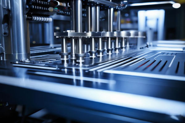
In the chip manufacturing process, key process steps such as plasma etching and Chemical Vapor Deposition (CVD) all require high-precision RF matching networks to ensure the stable generation and precise control of plasma. As chip process nodes continue to shrink, more stringent requirements are imposed on the performance indicators of RF matching networks, including matching accuracy, response speed, and power-carrying capacity.
Application Scenarios
Plasma Etching
RF matching networks ensure the stability of plasma density, enabling nanoscale precision etching to meet the requirements of advanced process nodes.
Chemical Vapor Deposition
Precisely control the deposition rate and film uniformity to ensure the high-quality construction of multi-layer chip structures.
Technical Advantages
The matching accuracy reaches 0.1%, ensuring plasma stability.
Response time is less than 10 microseconds, adapting to rapid process changes.
Supports wide frequency band operation from 13.56MHz to 60MHz
High power handling capability, with a continuous wave output of up to 3000W


 Home
Home Product
 Telephone
 Message


